
STEM
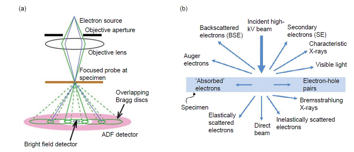
Scanning transmission electron microscopy was used in order to image the microsctructure of ABS. STEM combines both scanning electron microscopy (SEM) and transmission microscopy (TEM). Like the former, STEM focuses an electron beam on a very thin sample. These electrons interact with the atoms on the sample at various depths inside the sample.
Electrons pass through the sample and are collected by a transmission detector below the sample. Some electrons will however be absorbed by the material due to differences in composition or in thickness, therefore creating a contrasted image [1, 5].
But why use STEM and not conventional SEM or TEM ? On the one hand, STEM is preferred over SEM because of its improved spatial resolution. On the other hand, STEM is more user friendly than TEM and it is also possible to collect other of signals such as secondary electrons and back-scattered electrons. These signals cannot be spatially correlated in a conventional TEM, but can give another imaging mode in STEM [1,2].
There are two imaging mode in STEM: dark field and bright field. We will use the latter, as it is the most common one. In this mode, the contrast in the image is due to varying thickness or density inside the material. Denser or thicker areas will thus appear darker in the image, while lower density and thinner regions appear bright [1].
> How does it work ?
> Sample preparation
A sample of ABS was plunged in osmium tetroxide (OsO4 0.2%) for 3 days. Osmium tetroxide stained and hardened the unsaturated rubber phase of ABS. In fact, OsO4 reacts with the carbon double bond of polybutadiene. The heavy metal will increase the scattering of electrons in the rubber phase and enhance the contrast compared to the unstained matrix made of SAN. The rubber phase appears darker due to the scattering.
Besides staining, the osmium tetroxide also fixes the rubber phase. In fact, OsO4 creates a bridge (crosslinking) between polybutadiene chains which results in hardening.[3]
The reaction is shown below:
[2]

A 95 nm thick slice was cut with a diamond saw out from the stained ABS sample and used for imaging. Thanks to the hardening of the rubber phase, it was possible to cut it without tearing.
> Results
The sample was imaged with a JSM-7600F, JEOL Ltd, equipped with a transmission detector. We worked at 30 kV and with a bright-field detector.


[1] FEI, An Introduction to Electron Microscopy: The Scanning Transmission Electron Microscope, https://www.fei.com/introduction-to-electron-microscopy/stem/, consulted April 2017
[2] Katherine E. MacArthur, The Use of Annular Dark-Field Scanning Transmission Electron Microscopy for Quantitative Characterisation: A review of techniques developed for a high resolution study of bimetallic catalysts and other materials, Johnson Matthey Technol. Rev., 2016, 60, (2), 117, doi:10.1595/205651316x691186
[3] Linda C. Sawyer, Polymer Microscopy, Springer Science & Business Media, 2012, p.95
[4] D. M. KULICH, S. K. GAGGAR, V. LOWRY and R. STEPIEN, ACRYLONITRILE–BUTADIENE– STYRENE POLYMERS, ACRYLONITRILE AND ACRYLONITRILE POLYMERS (Vol 1), Encyclopedia of Polymer Science and Technology, p174-203
[5] ”Why STEM Not TEM”, http://www.spectral.se/spectral.nsf/f164f3e9b82f0febc1256dcc004611c1/d4a98a973f4e0290c12571e300376e06/$FILE/208%20Why%20STEM%20Not%20TEM.pdf, accessed 09/05/17
[6] Olagoke Olabisi and Kolapo Adewale, Handbook of Thermoplastics,CRC press, March 1997, p147
> Bibliography
According to Kulich et al [4] This corresponds to size of the rubber phase of ABS produced by emulsion process (200-400nm) [6]. The manufacturing process of our ABS is confirmed by the size of the SAN particules occluded in the rubber phase. In fact these are small compared to size of the rubber nodules [4].
It seems that there are two types of rubber phase, which two distinguishable sizes, in other words bimodal. This can be also noticed on the images shown by [6] which characterize ABS produced by emulsion process.
An explanation for the presence of a bimodal distribution of rubber phase is the combination of two fabrication processes, which is commonly used since a wide range of ABS products is possible with this technique. Bulk polymerization process is commonly used in combination with emulsion process. It leads to large nodules produced by bulk polymerization and smaller ones by emulsion process. Olagoke et al [6] shows, with the combination of processes, larges nodules of 200-400 nm and smaller ones ranging from 10 to 50 nm. This corresponds to our finding but is in contradiction with the sizes suggested by Kulich et al [6] (200-400 nm for emulsion and 1000-2000 nm for bulk polymerization).
In conclusion, our ABS is produced by a hybrid process.
By Elisabeth
By Roselien